CPR E 281x/282x - Lab 8a
1. Objectives
In this lab
you will use Verilog to design a SR Latch, D Latch, D
Flip-flop, 4-bit Register, and a 4-bit register with enable.
1.1
Reference Files for Lab
2. Prelab
Before you
come to lab it will be useful to become familiar with the different memory
elements. You will find information in
Chapter 7 of your text “Fundamentals of
Digital Logic with Verilog Design” by Brown and Vranesic.
3. SR Latch
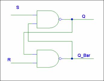
An SR
Latch is shown below. When S (set) and R
(reset) are both logical 1, the values on Q and Q_bar
remain the same as they were previously.
When S goes to logical 0, Q is set to 1 and Q_bar
is the complement. S can then go back to
logical 1, and the value at Q remains as logical 1. Likewise, when R goes to 0, Q will be set to
0, and Q_Bar is 1.
Write the Verilog code for the SR latch, SR_latch
(S,R,Q,Qbar), using the
same labels as the figure. Create a
waveform to test your design and observe the properties of the SR latch. What
happens when both S and R are set to zero?

4. D Latch
An SR latch can be used to store a value of a logical
variable. For this purpose, it is more useful if a clock (control) signal can
be used to trigger a change of state in Q and Q_bar
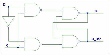
based on the value of the input variable, which we want to specify. A clocked latch is used for this purpose. In
a clocked latch, the outputs can change only when the inputs change AND the
clock is asserted (a logic 1 or logic 0, depending on type of logic used). In
the figure below, we show a clocked latch. In this figure when clock signal is
at logic 1, S and R input are asserted a set of values depending on the value
of D input. When clock signal is logic 0, both S and R are at logic 1, keeping
the old value of Q as it is.
Write the Verilog code for the
D-latch, D_latch(D, C, Q, Qbar),
shown below. Create a waveform that
demonstrates the proper functioning of your D latch.

5. D Flip-flop
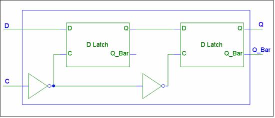
In contrast to a latch, the output of a flip-flop only
changes on a clock edge. The clock
edge which affects can be selected to be rising edge (clock signal going from 0
to 1) or falling edge, clock signal going from 1 to 0). This is realized using
the circuit shown below.
Create the Verilog code for the
rising-edge D-flip-flop, D_flipflop(D, C, Q, Qbar),
shown below by instantiating two D_latches and
associated circuitry. Notice that the circuit will be a falling-edge
D-flip-flop if the first NOT gate is removed.
Demonstrate the functioning of your D flip-flop with an appropriate
waveform.

6. 4-bit Register
Since we often work with data that is more than 1 bit wide,
it is useful to be able to store multiple bits at a time. A register
is a memory element that may store 1 or many bits of information, and is
basically just a collection of D flip-flops.
Write the Verilog code for a 4-bit
register, Reg4bit(D, C, Q), where D
and Q are 4-bit wide signals, i.e.
input [3:0] D; input C; and output [3:0] Q. Create a waveform that shows that the value
of Q only changes at the rising edge of the clock.
7. 4-bit Register with Enable
In the next lab we will be combining multiple registers
together to form a register file. In
order to do this, we need to be able to enable one of the registers, and
disable the rest. Thus, we will need to
add a 1 bit input, enable, to each
register. The performance of the
register with enable is as follows.
When enable is 0, the value of Q will always stay the same. When enable is a 1, the register will perform
as before, changing to the value of D at the edge of the clock.
Write the Verilog code for a 4-bit
register with enable, Reg4bitE(D, C, Q,
enable). HINT: Use a 2-to-1 Multiplexer to select the D input for each flip-flop,
with enable as the selection signal.