CPR E 381x/382x - Lab 2a
PC and
Memory Design
1. Objectives
In this lab you will design
modules for a simple datapath by designing a Program Counter (PC), Instruction
Memory, and Data Memory.
1.1 Reference Files for Lab
2. Prelab
Understand that a
microcontroller executes its program using a program counter that gets modified
each time an instruction is fetched, or a branch instruction is executed and
branch is taken, or a jump instruction is executed. That is why PC is
manipulated as shown here. Also, an instruction memory stores an instruction
that takes a full work in RISC type machines. Data Memory can read or write a
word or a byte of memory at atime.
3. Setup
Create
the folder in your home directory U:\CPRE381\Lab2a,
and then three sub-folders ~\PC, ~\InstrMem, ~\DataMem.
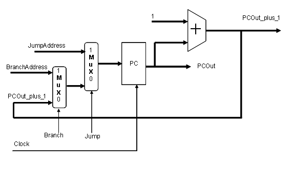
4. PC in Verilog
Program Counter (PC) is
basically an instruction address register that keeps track of the address of
the instruction, in the instruction memory, that is to be issued to the
Register File. It has the functionality of incrementing the instruction address
by one instruction, or selecting the branch address, or selecting the jump
address.
Design your PC module
according to the following schematic. The bus lines are all 32 bits wide.
5. Instruction Memory in Verilog
Design a word addressable
memory module that can be used for the Instruction Memory. The clock, MemWrite, and MemRead inputs are
1-bit wide, and all other inputs and outputs are 32-bits wide. The memory should be able to store 128 words,
thus, you will not use the full 32 bit address, as this would result in a 137
Gb memory. Instead, only use the least
significant bits of the address. The
memory should write the full 32-bit word, WriteData,
to the word specified by Address at
the negative edge of the clock if MemWrite
is asserted. ReadData outputs the data of the memory location specified by Address whenever MemRead is asserted.
Note: Because we are ignoring the most significant bits of the
address, we have created a wrap-around
instruction memory.

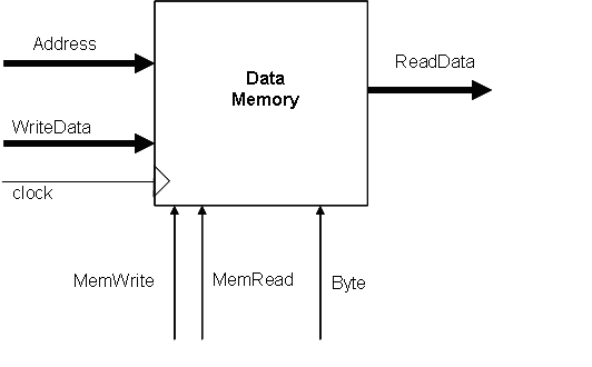
6. Data Memory in Verilog
Design a byte-addressable memory module that can be used for
data memory. The behavior of this module
will be similar to that of the instruction memory, with the addition of a byte signal that, when asserted,
specifies that only the byte given by Address[1:0]
should be read/written to. When writing only
a byte, the least significant byte of WriteData,
WriteData[7:0], should be written. When
reading only a byte, the byte specified should appear as the least significant byte
of ReadData, ReadData[7:0], and the
rest of the bits of ReadData should
be set to 0. Again, the size of the
memory should be 128 words.
To get started, design an 8-bit wide memory, capable of
storing 128 bytes. To implement the data
memory, you will use 4 of these memory blocks, one for each byte in the word,
as well as some basic modules (multiplexers, decoders, etc.) to decide which of
the memories should be written/read, and what data should be written/read.
Before you begin coding, draw a block diagram of your
byte-addressable memory and have it checked by the TA. It is helpful to think of reading and writing
separately, that is, first decide how you will implement the byte addressable
reads, then decide how you will implement byte addressable writes. Also, for the writing case, try to answer the
questions “What data is being written?” and “Where is it being written to?” These questions should be answered separately.
Note: To simplify design, you may
assume that all word reads and writes are word-aligned. That is to say, if byte = 0, then Address[1:0]
will be equal to 00. Also, note that we
are only implementing byte and word data, not half-word data.